Tuesday, November 23, 2010
Tuesday, November 16, 2010
Monday, November 8, 2010
Combining Nanotechnology and Textile Technology to make Superior Buckypaper
| Combining nanotechnology and textile technology to make superior buckypaper | |
| (Nanowerk Spotlight) While individual carbon nanotubes could find applications in nanoelectronics, in order to exploit their intriguing properties on the macroscale, for instance in thin films and membranes, many trillions of these tubes must be assembled. These macroscopic aggregates are commonly called buckypapers – thin sheets made from intertwined carbon nanotubes (CNTs). | |
| Buckypapers could find numerous applications: As one of the most thermally conductive materials known, buckypaper could lead to the development of more efficient heat sinks for chips; a more energy-efficient and lighter background illumination material for displays; a protective material for electronic circuits from electromagnetic interference due to its unusually high current-carrying capacity; or switchable surfaces (see: "Nanotechnology paper for switchable surfaces"). | |
| To date, CNT membranes are mainly prepared using an ancient art of paper making, namely, via the filtration of CNT suspensions in water and then drying of the resulting slurry. A number of alternative fabrication methods of CNT membranes have also been reported, namely solid-state drawing, spin coating, drop casting, dip casting, and Langmuir-Blodgett deposition. However, these methods have limitations including poor film homogeneity and uniformity, difficult thickness and structure control, and/or low production efficiency, and hence the resultant CNT membranes or buckypapers have not realized the potential mechanical, electrical, and optical properties that individual CNTs can provide. | |
| Borrowing a technology from the textile industry, researchers have developed a novel nanotechnology fabrication technique that results in high-quality CNT membranes with controllable thickness and topology at high-speed and low-cost for many practical applications. | |
| "Our hydroentangling method is the result of converging two completely different fields, i.e., nanotechnology and modern textile technology, and can revolutionize the way we make nanomaterials" Dr. Xiangwu Zhang tells Nanowerk. "Our hydroentangled CNT membranes have significantly greater mechanical and electrical properties than the state-of-the-art CNT buckypapers made from filtration." | |
 | |
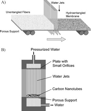
| Hydroentangling of CNTs: A) Schematic of the continuous hydroentangling process that can produce hydroentangled nonwovens at a speed up to 400 meters per minute. B) Schematic of the bench-top hydroentangling setup that can produce batches of hydroentangled CNT membranes. (Reprinted with permission from Wiley) | |
| Zhang, an Assistant Professor in the College of Textiles at North Carolina State University, explains that hydroentangling, also known as hydraulic needling, is a relatively new, simple, high-speed, low-cost, environmentally benign process for mechanically bonding fibers to form a strong and uniform nonwoven fabric or membrane. | |
| In the October 6, 2008 online edition of Advanced Materials, Zhang describes how he used the hydroentangling phenomenon to assemble individual CNTs into strong, electrically-conducting, multifunctional CNT membranes ("Hydroentangling: A Novel Approach to High-Speed Fabrication of Carbon Nanotube Membranes"). | |
| "Using hydroentangling to assemble CNTs is extremely simple and super fast" he says. "The resulting membranes have significantly greater mechanical and electrical properties than the state-of-the-art CNT buckypapers made from filtration. In addition, these CNT membranes maintain all the multifunctional properties of individual CNTs, and hence they have many potential applications such as field emission displays, catalyst supports, biomedical electronics, solar collection, hydrogen storage, sensors, fuel cells, and batteries." | |
| Zhang points out that, unlike other traditional textile processes that deal with individual fibers or yarns, hydroentangling treats the stack of unentangled fibers as a whole to produce strong fabrics or membranes, and hence it is an excellent method to assemble CNTs, which are too small to be manipulated individually. The continuous hydroentangling process used in the textile industry is able to produce nonwovens at a speed up to 400 meters per minute. | |
| In Zhang's work, his team assembled a bench-top hydroentangling setup to prepare CNT membranes. "Using this setup, we completed the hydroentangling of CNTs between 5 seconds and 2 minutes, depending on the membrane thickness" he says. "The resultant membranes have a diameter of 25 millimeters. The fabrication of CNT membranes with larger sizes can be realized using the continuous process or a bench-top setup with a larger-diameter support." | |
 | |
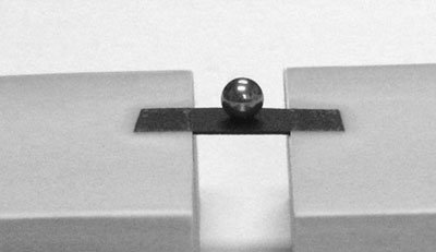
| Photograph showing a hydroentangled CNT membrane supporting a stainless steel ball, where the mass of the steel ball is about 10 000 times that of the contacting membrane region. The hydroentangled CNT membrane was attached to two blocks using transparent tape. (Reprinted with permission from Wiley) | |
| Interestingly, Zhang demonstrated that the tensile strength of hydroentangled CNT membrane with a thickness of 100 µm is 51 MPa, which is three times greater than that of filtration-produced CNT buckypaper. | |
| "By infiltrating polymers into hydroentangled CNT membranes, we can obtain CNT-based polymer composites with even higher mechanical properties" says Zhang. "For example, the introduction of polyethylene oxide (PEO) into hydroentangled CNT membrane can increase the strength by 37%, which indicates that PEO chains can minimize the nanotube slippages and stabilize the entanglements during the tensile loading." | |
| Zhang cautions that, although his team has successfully demonstrated high-performance hydroentangled CNT membranes, they still do not completely understand what really happens during the CNT hydroentangling process. This of course is a prerequisite of commercial applications of this process and therefore Zhang's team is making this a focus of their further research. | |
| By Michael Berger. Copyright 2008 Nanowerk LLC |
Tuesday, November 2, 2010
Monday, October 25, 2010
CNT OLEDs
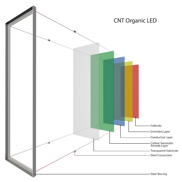
Researchers in Canada have demonstrated OLEDs based on carbon nanotube anodes that are as efficient as comparable indium tin oxide (ITO) devices. While this part seems to be only JUST equal, there are several advantages that the CNTs provide, such as increased material flexibility and hardiness. This could make them an attractive alternative to transparent conducting oxides for OLEDs.
Amazingly, many researchers say this method of creating OLEDs with CNTs is cheaper than using ITO. Another current limitation of OLEDs is the transistors that the electric currents run along. Right now, the current has to run ALONG the transistors, which means that for the OLED to be bright, and visible, the display has to be small. Many Android smart phones are beginning to employ OLED screens. This is the extent though. OLEDs made with ITO are also, fragile, somewhat rigid and one sided. By applying the appropriate chemical treatment, nanotubes could also replace the metal cathodes found in OLEDs. This would allow the devices to emit light from both sides. Not to mention that the OLEDs would be completely transparent, and as thin as 1 to 8 mm.
Another similar development in CNT OLEDs comes from The University of Southern California Viterbi School of Engineering. USC is one of many groups around the world trying to perfect the technology in applications such as affordable "head-up" car windshield displays; eyeglasses to watch videos for when you are sitting in an airport or train station and ultra thin, low-power "e-paper" capable of full color motion video.
Chongwu Zhou of USCs Ming Hsieh Department of Electrical Engineering has been working on transparent electronics for the past three years and last year developed a prototype devices in which transparent electronics were built on top of a flexible transparent base. This was accdomplished using carbon nanotubes. Earlier attempts at transparent devices used other semiconductor materials with disappointing electronic results, enabling one kind of transistor (n-type); but not p-types; both types are needed for most applications.
The critical improvement in performance, according to the research, came from the ability to produce extremely dense, highly patterned lattices of nanotubes, rather than random tangles and clumps of the material. These new aligned nanotube transistors are easy to fabricate and integrate, as compared to individual nanotube devices. The transfer printing process allows the devices to be fabricated through low temperature processes, which is important for realizing transparent electronics on flexible substrates.
Zhou believes that we may be 2 to 6 years away from mass production of transparent electronics. One barrier is the inertia of old existing technology.
NOTE: Samsung has released the first nanotube based OLED screen called "BluePhase".
Tuesday, October 19, 2010
Presentation 10/19/10: Nanotube Composite: OPVs
Currently, photovoltaics are a new trend in the production of cheap, clean, and green energy. There are multiple ways of producing a photovoltaic, however, one thing remains a hindrance that limits the desire for photovoltaics. Efficiency. A standard photovoltaic cell currently operates at an efficiency of 1-3%. Remarkably, this is not a small amount of energy. Unfortunately, to produce enough energy using only photovoltaics, the ratio of size to received energy is not feasible. Very large arrays of photovoltaics are needed to produce large quantities of energy. Therefore, intense research is being conducted to increase the efficiency of photovoltaics.
One of the key developments is a nanotube suspension (Buckypaper) in a polymer to produce a photovoltaic at up to 15 times more efficient, and potentially up to 50 times more efficient.
Initial addition of carbon nanotubes to photovoltaics give them a new name: Organic photovoltaic devices (OPVs). They are fabricated from thin films of organic semiconductors, such as polymers and small-molecule compounds, and are typically around 100 nm thick. Because polymer based OPVs can be made using a coating process such as spin coating or inkjet printing, they are an attractive option for inexpensively covering large areas as well as flexible plastic surfaces. A promising low cost alternative to silicon solar cells, there is a large amount of research being dedicated throughout industry and academia towards developing OPVs and increasing their power conversion efficiency.
In Short, indium tin oxide (ITO) is the primary suspended conductor in a photovoltaic. This is the substance that conducts the solar rays into energy for use. The problem with this material is that it is brittle and not very efficient. It is until now the most efficient material used. Nanotubes, though increadibly strong, allow the material to become flexible and very thin. Of course, the efficiency is over times time more than what is currently used.
Also, Due to the simple fabrication process, low production cost, and high efficiency, there is significant interest in dye-sensitized solar cells (DSSCs). Currently, using ITO technology, dyed cells can convert energy at a rate of 11%. Using nanotubes, this coversion rate can be increased up to 50%. This is even newer technology and is still under development.
One of the key developments is a nanotube suspension (Buckypaper) in a polymer to produce a photovoltaic at up to 15 times more efficient, and potentially up to 50 times more efficient.
Initial addition of carbon nanotubes to photovoltaics give them a new name: Organic photovoltaic devices (OPVs). They are fabricated from thin films of organic semiconductors, such as polymers and small-molecule compounds, and are typically around 100 nm thick. Because polymer based OPVs can be made using a coating process such as spin coating or inkjet printing, they are an attractive option for inexpensively covering large areas as well as flexible plastic surfaces. A promising low cost alternative to silicon solar cells, there is a large amount of research being dedicated throughout industry and academia towards developing OPVs and increasing their power conversion efficiency.
Also, Due to the simple fabrication process, low production cost, and high efficiency, there is significant interest in dye-sensitized solar cells (DSSCs). Currently, using ITO technology, dyed cells can convert energy at a rate of 11%. Using nanotubes, this coversion rate can be increased up to 50%. This is even newer technology and is still under development.
Monday, September 20, 2010
Tuesday, September 14, 2010
Monday, September 13, 2010
Carbon Nanotube Composites
Carbon Nanotubes are a new technology for making Smart Composites.
http://www.personal.rdg.ac.uk/~scsharip/IMR3.pdf
http://www.personal.rdg.ac.uk/~scsharip/IMR3.pdf
Subscribe to:
Comments (Atom)


