


| Combining nanotechnology and textile technology to make superior buckypaper | |
| (Nanowerk Spotlight) While individual carbon nanotubes could find applications in nanoelectronics, in order to exploit their intriguing properties on the macroscale, for instance in thin films and membranes, many trillions of these tubes must be assembled. These macroscopic aggregates are commonly called buckypapers – thin sheets made from intertwined carbon nanotubes (CNTs). | |
| Buckypapers could find numerous applications: As one of the most thermally conductive materials known, buckypaper could lead to the development of more efficient heat sinks for chips; a more energy-efficient and lighter background illumination material for displays; a protective material for electronic circuits from electromagnetic interference due to its unusually high current-carrying capacity; or switchable surfaces (see: "Nanotechnology paper for switchable surfaces"). | |
| To date, CNT membranes are mainly prepared using an ancient art of paper making, namely, via the filtration of CNT suspensions in water and then drying of the resulting slurry. A number of alternative fabrication methods of CNT membranes have also been reported, namely solid-state drawing, spin coating, drop casting, dip casting, and Langmuir-Blodgett deposition. However, these methods have limitations including poor film homogeneity and uniformity, difficult thickness and structure control, and/or low production efficiency, and hence the resultant CNT membranes or buckypapers have not realized the potential mechanical, electrical, and optical properties that individual CNTs can provide. | |
| Borrowing a technology from the textile industry, researchers have developed a novel nanotechnology fabrication technique that results in high-quality CNT membranes with controllable thickness and topology at high-speed and low-cost for many practical applications. | |
| "Our hydroentangling method is the result of converging two completely different fields, i.e., nanotechnology and modern textile technology, and can revolutionize the way we make nanomaterials" Dr. Xiangwu Zhang tells Nanowerk. "Our hydroentangled CNT membranes have significantly greater mechanical and electrical properties than the state-of-the-art CNT buckypapers made from filtration." | |
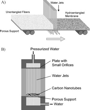 | |
| Hydroentangling of CNTs: A) Schematic of the continuous hydroentangling process that can produce hydroentangled nonwovens at a speed up to 400 meters per minute. B) Schematic of the bench-top hydroentangling setup that can produce batches of hydroentangled CNT membranes. (Reprinted with permission from Wiley) | |
| Zhang, an Assistant Professor in the College of Textiles at North Carolina State University, explains that hydroentangling, also known as hydraulic needling, is a relatively new, simple, high-speed, low-cost, environmentally benign process for mechanically bonding fibers to form a strong and uniform nonwoven fabric or membrane. | |
| In the October 6, 2008 online edition of Advanced Materials, Zhang describes how he used the hydroentangling phenomenon to assemble individual CNTs into strong, electrically-conducting, multifunctional CNT membranes ("Hydroentangling: A Novel Approach to High-Speed Fabrication of Carbon Nanotube Membranes"). | |
| "Using hydroentangling to assemble CNTs is extremely simple and super fast" he says. "The resulting membranes have significantly greater mechanical and electrical properties than the state-of-the-art CNT buckypapers made from filtration. In addition, these CNT membranes maintain all the multifunctional properties of individual CNTs, and hence they have many potential applications such as field emission displays, catalyst supports, biomedical electronics, solar collection, hydrogen storage, sensors, fuel cells, and batteries." | |
| Zhang points out that, unlike other traditional textile processes that deal with individual fibers or yarns, hydroentangling treats the stack of unentangled fibers as a whole to produce strong fabrics or membranes, and hence it is an excellent method to assemble CNTs, which are too small to be manipulated individually. The continuous hydroentangling process used in the textile industry is able to produce nonwovens at a speed up to 400 meters per minute. | |
| In Zhang's work, his team assembled a bench-top hydroentangling setup to prepare CNT membranes. "Using this setup, we completed the hydroentangling of CNTs between 5 seconds and 2 minutes, depending on the membrane thickness" he says. "The resultant membranes have a diameter of 25 millimeters. The fabrication of CNT membranes with larger sizes can be realized using the continuous process or a bench-top setup with a larger-diameter support." | |
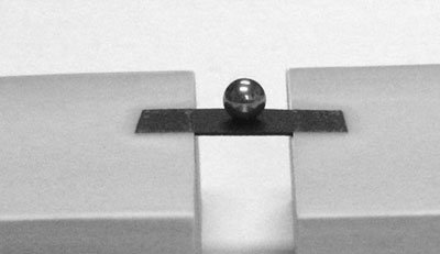 | |
| Photograph showing a hydroentangled CNT membrane supporting a stainless steel ball, where the mass of the steel ball is about 10 000 times that of the contacting membrane region. The hydroentangled CNT membrane was attached to two blocks using transparent tape. (Reprinted with permission from Wiley) | |
| Interestingly, Zhang demonstrated that the tensile strength of hydroentangled CNT membrane with a thickness of 100 µm is 51 MPa, which is three times greater than that of filtration-produced CNT buckypaper. | |
| "By infiltrating polymers into hydroentangled CNT membranes, we can obtain CNT-based polymer composites with even higher mechanical properties" says Zhang. "For example, the introduction of polyethylene oxide (PEO) into hydroentangled CNT membrane can increase the strength by 37%, which indicates that PEO chains can minimize the nanotube slippages and stabilize the entanglements during the tensile loading." | |
| Zhang cautions that, although his team has successfully demonstrated high-performance hydroentangled CNT membranes, they still do not completely understand what really happens during the CNT hydroentangling process. This of course is a prerequisite of commercial applications of this process and therefore Zhang's team is making this a focus of their further research. | |
| By Michael Berger. Copyright 2008 Nanowerk LLC |
 Many corporations and researchers have been investing a lot of money in the development of OLEDs.


